Chapter 4 Sequential Logic
Storage Elements and Sequential Circuit Analysis
Types of Sequential Circuits
Synchronous
- Behavior defined from knowledge of its signals at discrete instances of time
- Storage elements observe inputs and can change state only in relation to a timing signal (clock pulses from a clock)
Asynchronous
-
Behavior defined from knowledge of inputs an any instant of time and the order in continuous time in which inputs change
-
If clock just regarded as another input, all circuits are asynchronous!
-
Nevertheless, the synchronous abstraction makes complex designs tractable!
Circuit Delay Model


Latches
- Long term maintaining a given stable state
- There are two stable states, "0", "1"
- Under certain conditions, can change state at anytime
Basic(NAND) \(\bar{S}-\bar{R}\) Latch

- So RS state 00 is forbidden!
Basic(NOR) \(S-R\) Latch

- So RS state 11 is forbidden!

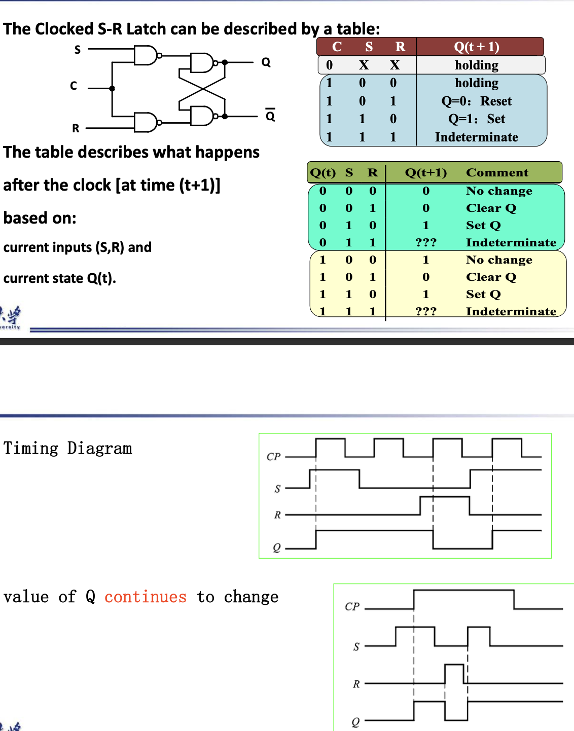
Clocked S-R Latch
- Adding two NAND gates to the basic S - R NAND latch gives the clocked S – R latch
- Has a time sequence behavior similar to the basic S-R latch except that the S and R inputs are only observed when the line C is high.
Details
D Latch
- Adding an inverter to the S-R Latch, gives the D Latch -- No indeterminate states

| Q | D | Q(t+1) | Comment |
| 0 | 0 | 0 | No Change |
| 0 | 1 | 1 | Set Q |
| 1 | 0 | 0 | Clear Q |
| 1 | 1 | 1 | No Change |
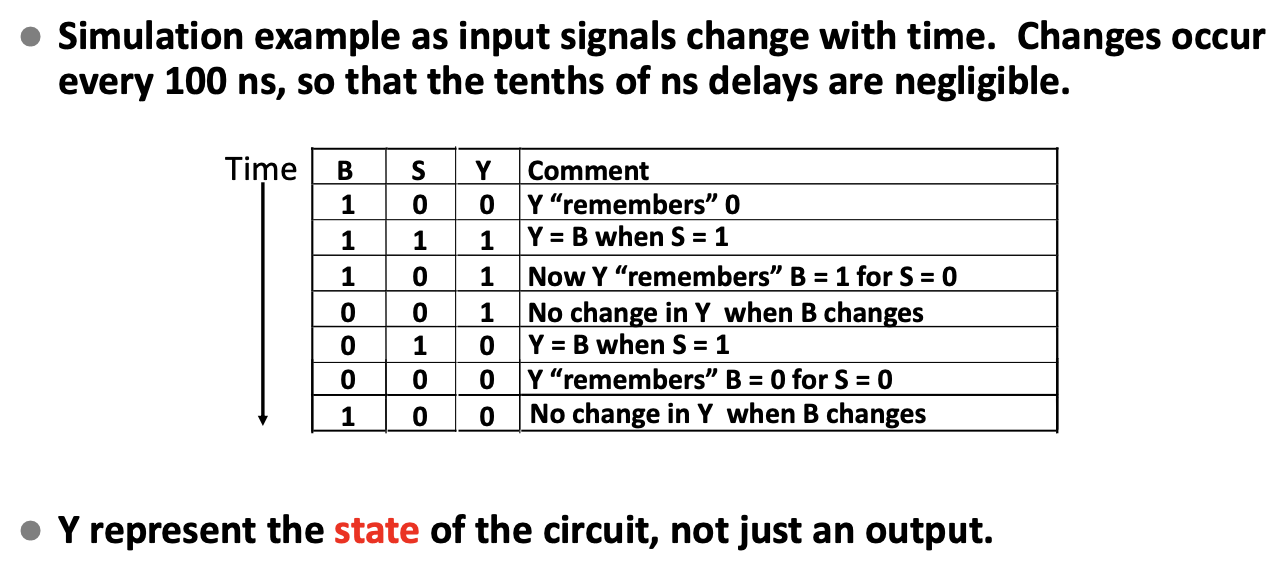
The Latch Timing Problem

- We CANNOT be sure what value will Y output when C=0
- This is the Latch Timing Problem.
- In one Clock Pulse, Y can change many times if the Input Changes.
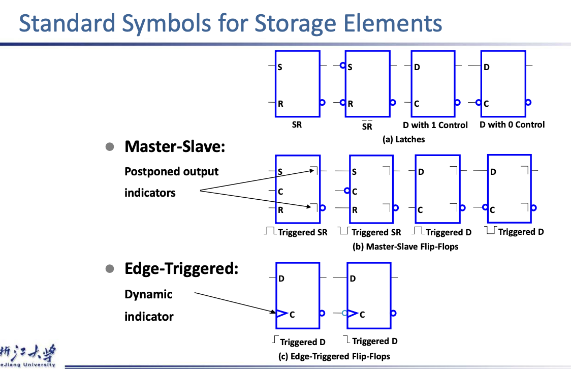
Flip-Flops
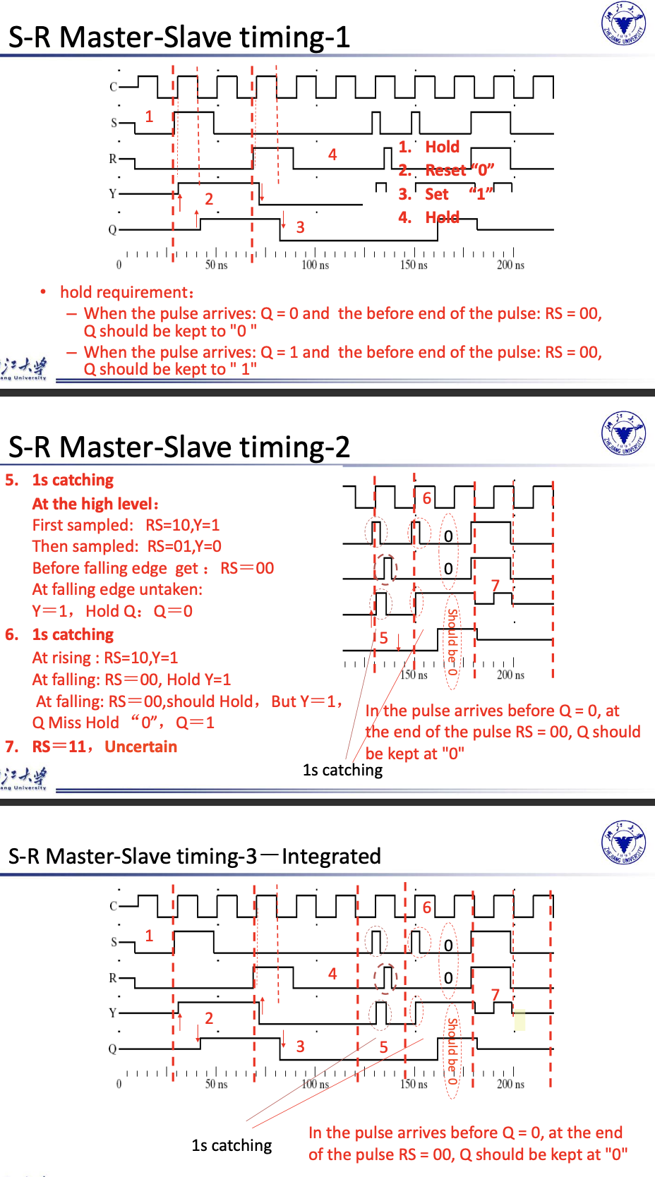
S-R Master-Slave Flip-Flop

- The Problem of 1s Catching
While \(C=1\) \(S\) \(and/or\) \(R\) are permited to change.
- Suppose \(Q\) =\(0\) and \(S\) goes to \(1\) and then back to \(0\) with \(R\) remaining at \(0\)
The master latch sets to \(1\)
A \(1\) is transferred to the slave
- Suppose \(Q\) = \(0\) and \(S\) goes to \(1\) and back to \(0\) and \(R\) goes to \(1\) and back to \(0\)
The master latch sets and then resets
A \(0\) is transferred to the slave
- Personally main problem: The hold state when \(S=R=0\)
Details
Edge-Triggered D Flip-Flop
- The delay of the S-R master-slave flip-flop can be avoided since the 1s-catching behavior is not present with D replacing S and R inputs
- The change of the D flip-flop output is associated with the negative edge at the end of the pulse
- It is called a negative-edge triggered flip-flop


Flip-Flop Timing Parameters
- \(t_s\) -- Setup Time
Master-slave - Equal to the width of the triggering pulse (Because of the 1's Catching the triggering pulse once arrives is forbidden to change)
Edge-triggered - Equal to a time interval that is generally much less than the width of the the triggering pulse
-
\(t_h\) Hold Time -- often equal to zero
-
\(t_w\) Clock Pulse Width
-
\(t_{px}\)
Same parameters as for gates except that measured from clock edge that triggers the output change to the output change.
More Specifically
- 这几个时间点起点/终点都是触发边缘;
- Propagation Time 一定长于 Hold Time,因此在计算电路延迟时只考虑 Propagation Time;
- Pulse-trigger 和 Edge-trigger 在表现上的区别在于 Setup Time,前者需要覆盖整个 pulse(
posorneg);

Summary
Sequential Circuit Design
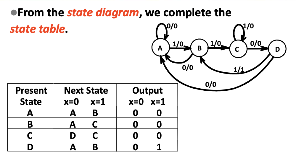
State Table
State Diagrams
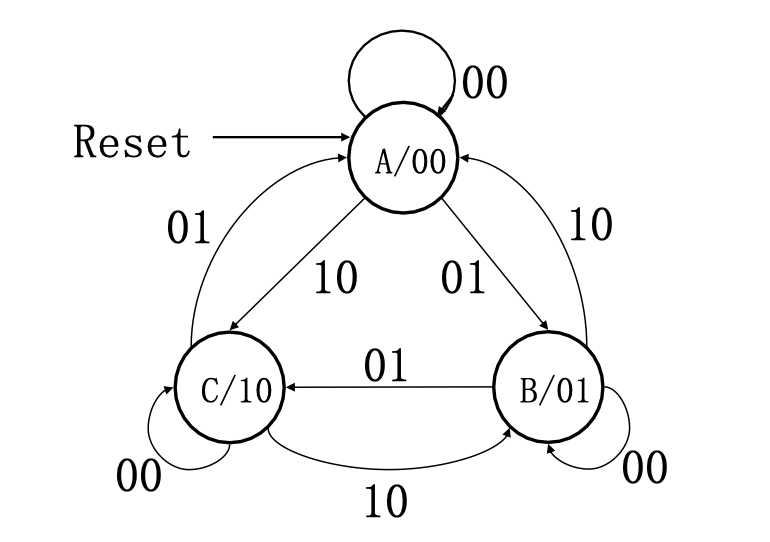
Moore Models
Outputs are a function ONLY of states
Mealy Models
Outputs are a function of inputs AND states
Details


Equivalent State

Circuit and System Level Timing
- \(t_p\) clock period --The interval between occurrences of a specific clock edge in a
periodic clock
- \(t_{pd,COMB}\) -- total delay of combinational logic along the path from flip-flop output to
flip-flop input
- \(t_{slack}\) -- extra time in the clock period in addition to the sum of the delays and
setup time on a path : Must be greater than or equal to zero on all paths for correct operation
- \(t_{pd,FF}\) -- Flip-Flop's delay

- Timing Equations
\(t_p=t_{slack}+(t_{pd,FF}+t_{pd,COMB}+t_s)\)
\(t_{stack}\) must be greater than or equal to zero so \(t_{p} \ge max(t_{pd,FF}+t_{pd,COMB}+t_s)\)
from all paths from flip-flop output to flip-flop input
-
Can be calculated more precisely by using \(t_{PHL}\) and \(t_{PLH}\) values instead of \(t_{pd}\) values, but requires consideration of inversions on paths
-
Calculation[Refer to PPT]
Example Recognize 1101


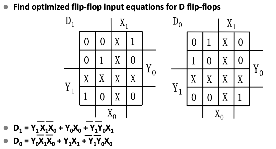
State Assignment
- Each of the m states must be assigned a unique code
- Minimum member of bits required is n such that \(n\ge[log_2m]\)
The task of state assignment involves determining the encoding length and finding an optimal (often challenging) or near-optimal state assignment scheme, leading to different expressions for output functions and activation functions, and consequently varying circuit complexities. The basic principles of state assignment are:
- Determine the length of the encoding.
- Seek an optimal (difficult to find) or near-optimal state assignment scheme.
The fundamental principles of assignment are as follows:
- Under the same input conditions, states with the same next states should preferably be assigned adjacent binary codes.
- Under adjacent input conditions, the next states of the same current state should preferably be assigned adjacent binary codes.
- Current states with identical outputs should preferably be assigned adjacent binary codes.
- Minimize the occurrence of the most frequently appearing states in the state table, or assign logic 0 to initial states.
Generally, the first principle is of greater importance and should be prioritized. Subsequently, consideration should be given to the frequency of occurrence of state pairs resulting from the first three principles, with a preference for assigning adjacent binary codes to state pairs with higher frequencies.
-
EXAMPLE -- Refer to the PPT
-
Design a sequential modulo 3 accumulator for 2-bit operands
Details


Other Flip-Flop Types
J-K Flip-Flop
Same as S-R flip-flop with J analogous to S and K analogous to R
- J=K=1 is allowed ; the flip-flop changes to opposite state
- As a master-slave, has same “1s catching” behavior as S-R flip-flop
- To avoid 1s catching behavior,one solution used is to use an edge-triggered D as the core of the flip-flop

T Flip-flop
Has a single input T
- For T = 0, no change to state
- For T = 1, changes to opposite state
Same as a J-K flip-flop with J = K = T
- As a master-slave, has same “1s catching” behavior as J-K flip-flop
-
Cannot be initialized to a known state using the T input
-
To avoid 1s catching behavior,one solution used is to use an edge-triggered D as the core of the flip-flop

Basic Flip-Flop Descriptors
- Characteristic Table
- Excitation Table
Eg.


Flip-Flop Behavior Example


创建日期: 2024年1月2日 12:12:25